There have been numerous difficulties understanding strange behaviors when setting various configurations of the PRCI clock path of the FE310 SoC. These difficulties arise from two errors in the circuit diagram shown in Figure 2 of Section 6 of version 1p4 of the Manual.
-
pllbypassmux ‘0’ input connects to output ofpllrefselmux, not the HFX clock source -
pllselmux ‘1’ input connects to output ofpllbypassmux, not the PLL output
The diagram as shown in the Manual is below:
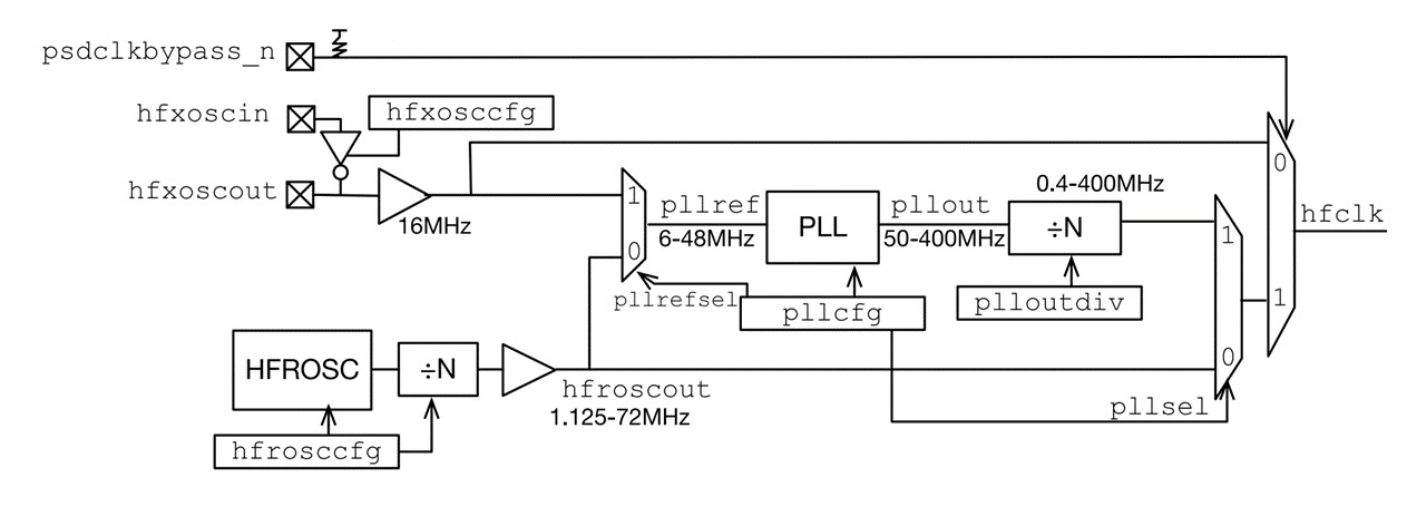
The correct diagram is shown below:

One of the clues, explaining (1), is a paragraph of Section 6.5:

The other clue is the fact that, when PLL is turned off (by pllbypass=1), the pllsel is able to control whether hfclk is driven only by HFR or by the selection of pllrefsel.
A few general rules that I discovered, that result in reliable and smooth operation:
- Change
pllrefselonly whenpllbypass=1 (PLL off) to prevent PLL unlock and possible latch-up - Set
pllbypass=0 (PLL on) only when HFR is enabled andpllsel=0, to allow PLL settle and give time to acquire lock condition - Change
pllrefselonly when HFR is enabled andpllsel=0, to prevent possible latch-up
Some of the earlier discussions related to this topic are
FE310-G002 v1p0 manual errata (@pete_buechler @JimWilson),
Is it possible to brick the HiFive board? (@dvc @mwachs5
@brucehoult),
Unable to read PRCI registers (@c0ntrarian @pds),
Clock generation and configuration (@stef), and
Dtmcontrol_scan stuck in infinite loop (@tim @pds).


