What is PLIC interrupt source start and end in interrupt source mapping?

FE310-G002 manual for PLIC has the Table 24: PLIC Interrupt source mapping. I don’t understand the source start and source end. For example GPIO interrupt is a source, but what is start and end value (8, 39) & how are these used?

To enable GPIO interrupt, I enable bit 8 (PLIC interrupt enable register 1). right? where should 39 be used?

Each of the PLIC interrupt sources are in a packed format in the Enable and Pending registers. Each bit in the register is one of the interrupt sources.

The Enable and Pending registers are each 64-bits long; think about them as sets of two 32-bit registers, an upper word and a lower word.

Their register word index is the PLIC interrupt source number divided by 32 (integer-wise; i.e., truncated or rounded-down).

The register bit position is the PLIC interrupt source number modulus 32 (i.e., the remainder of division; see RISC-V instruction remu).

There is no PLIC interrupt source ‘0’, and the least significant (right-most) bit position #0 similarly reflects this.

Lower register word

AON : start=1 end=2

  aon_wdt plic source id 1  (register bit position 1)
  aon_rtc plic source id 2

UART : start=3 end=4

  uart0   plic source id 3
  uart1   plic source id 4

SPI : start=5 end=7

  qspi0   plic source id 5
  spi1    plic source id 6
  spi2    plic source id 7

GPIO : start=8 end=39

  gpio0   plic source id 8
  gpio1   plic source id 9
  gpio2   plic source id 10
  gpio3   plic source id 11
  gpio4   plic source id 12
  gpio5   plic source id 13
  gpio6   plic source id 14
  gpio7   plic source id 15
  gpio8   plic source id 16
  gpio9   plic source id 17
  gpio10  plic source id 18
  gpio11  plic source id 19
  gpio12  plic source id 20
  gpio13  plic source id 21
  gpio14  plic source id 22
  gpio15  plic source id 23
  gpio16  plic source id 24
  gpio17  plic source id 25
  gpio18  plic source id 26
  gpio19  plic source id 27
  gpio20  plic source id 28
  gpio21  plic source id 29
  gpio22  plic source id 30
  gpio23  plic source id 31  (register bit position 31)

Upper register word

  gpio24  plic source id 32  (register bit position 0)
  gpio25  plic source id 33
  gpio26  plic source id 34
  gpio27  plic source id 35
  gpio28  plic source id 36
  gpio29  plic source id 37
  gpio30  plic source id 38
  gpio31  plic source id 39

PWM : start=40 end=51

  pwm0_0  plic source id 40
  pwm0_1  plic source id 41
  pwm0_2  plic source id 42
  pwm0_3  plic source id 43
  pwm1_0  plic source id 44
  pwm1_1  plic source id 45
  pwm1_2  plic source id 46
  pwm1_3  plic source id 47
  pwm2_0  plic source id 48
  pwm2_1  plic source id 49
  pwm2_2  plic source id 50
  pwm2_3  plic source id 51

I2C : start=52 end=52

  i2c     plic source id 52  (register bit position 20)

@pds Thanks for the elaborate reply and this details should go to manual too.

Further, the manual also don’t have much information on GPIO drive strength. Do you know the VALID range for ds (0x10012014) register? The manual just say each pin has a software controllable drive strength & not much about the value range and the corresponding current output.

Appreciated @bsvtgc glad it helps.

I’ve found the Datasheet to be a very useful companion to the Manual that you mention. Another handy resource is the Core Complex Manual, which has specifics of the ISA instructions as well as programming flow, boot processes, and interrupts. Sometimes, undocumented features and behaviors can be found in the actual circuit design of the SoC in sifive-blocks; for example, in case of SPI peripheral, the register EXTRADEL at offset 0x38, and SAMPLEDEL at offset 0x3C.

Table 4.2 in the Typical Electrical Specifications of the Datasheet tells us what are the GPIO pin Drive Strengths.

Thus, each of the 32 bits of ds (0x10012014), one for each pin, are

0=1ma, 1=20ma

Each of the 32 bits of pue (0x10012010) are

0=open-drain, 1=push-pull

The schematic diagram of a GPIO pin in Chapter 16, Figure 9 of the Manual is also very helpful in this case, and for understanding the direct external and the IOF internal pin control modes in general. For example, OUT_XOR operates on a pin regardless of mode; while the interrupt input enable and pending settings RISE, FALL, HIGH, and LOW (unfortunately) only operate in the direct external mode.


I might suggest, unless you need the speed or fast transition of an output pin, to use the lowest DS setting. In this way, you would save a pin from being accidentally and permanently destroyed in case of two or more 20mA strong drive outputs in push-pull mode being tied together, or an output inadvertently being shorted to ground or power.

@pds

Thanks for the mention of data sheet. I have been looking these electrical details.

Following is how I use GPIO now:

Configure GPIO 21 as output, (retaining ds & due registers as unchanged ( value 0)).

In schematics, Blue LED is connected between GPIO21 & VDD 3.3 through 330 ohm resistor.
So writing “1” to GPIO 21 would switch OFF the LED and “0” would switch ON the LED.

In this case, the current (3.3 / 330) would be drained from the VDD 3.3 src safely.
I tested and GPIO 21 worked as expected except that the rise interrupt is NOT getting triggered. Do you see any harm in this way of use?

Regarding the rise interrupt not getting triggered,
I confirmed the mtvec is in direct mode, trap routine mapped, machine external interrupt enabled (0x800) in mie register, plic interrupt enabled for source id 29, ((gdb) x *0x0c002000 0xfffd7eee). GPIO21 is configured with as output only. Am I missing something?

I ask as I read on your statement above " settings RISE , FALL , HIGH , and LOW (unfortunately) only operate in the direct external mode"

Could you please elaborate on “direct external mode”?

@bsvtgc everything seems well and good – I confirmed it with hardware and scope.

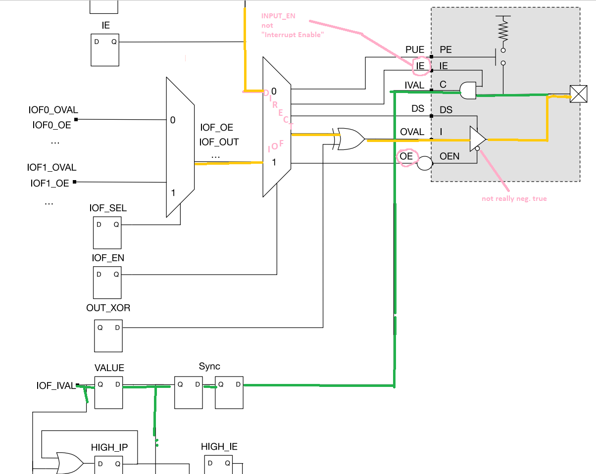
For interrupts to be sensed properly, the input enable bit for that pin must be set; otherwise, you won’t see any triggering. The INPUT_EN (0x10012004) register enables both the reading of a pin’s level, and the sensing of its levels and/or edges.

If you are internally driving the pin, the corresponding output enable bit for that pin must also be set, in addition to the input enable bit. The OUTPUT_EN (0x10012008) register enables the signal path out to the pin. Of course, if you are externally driving the pin, the output enable bit for that pin must not also be set.

Sketched below on Figure 9 of Chapter 16 of the Manual is the entire signal flow path, followed by the way I set up the code:

Route the path:

gpio_input_en |= (1UL << 21);  // req'd for sensing interrupt
gpio_output_en |= (1UL << 21);  // internal control, no external driving source connected

Enable the interrupt as you’ve done, and which I do in this order: mtvec, PLIC_PRIORITY (0=off, 1=lowest, 7=highest; written to 0x0C000000 + 4 * source_id), PLIC_ENABLE (set bit source_id % 32; of 0x0C002000 + 4 * (source_id/32)), PLIC_THRESHOLD (0=permit all, 7=mask all; written to 0x0C200000), interrupt source (i.e., CSR_MIE_MEIE) of mie, and the interrupt enable (i.e., CSR_MSTATUS_MIE) of mstatus.

Pick one, or more, sensing mode(s) as desired:

gpio_rise_ie = (1UL << 21);
gpio_fall_ie &= ~(1UL << 21);
gpio_high_ie &= ~(1UL << 21);
gpio_low_ie &= ~(1UL << 21);

Trigger the event:

  while(1)
  {
    gpio_output_val |= (1UL << 21);  // high
    gpio_output_val &= ~(1UL << 21);  // low
  }

Handle the interrupt. In case of GPIO direct external mode (i.e., ‘GPIO’ mode, by which I mean non-IOF functions, when the IOF_EN bit for that pin is set to 0), you must manually clear the pending interrupt before the handler returns. Otherwise, you will see a never-ending stream of interrupts back to the same handler. For the GPIO block, clear the _IP pending bits by setting them, rather than clearing them.

Some time during the handling process, either before or after your code, you need to CLAIM the interrupt, by reading the value from 0x0C200004, and writing it back to the same register. I read the claim value before my code, save it on the stack, and write it back after my code, as suggested in the RISC-V documentation.

.equ GPIO_BASE, 0x10012000
.equ GPIO_RISE_IP, 0x1C
.equ GPIO_FALL_IP, 0x24
.equ GPIO_HIGH_IP, 0x2C
.equ GPIO_LOW_IP,  0x34

plic_gpio21:  # plic source id 29
  # your stuff goes here ...

  # set to '1' the corresponding interrupt pending bit
  # to clear the trigger mode(s) you have enabled
  lui t0, %hi(GPIO_BASE)
  addi t2, t2, 1
  slli t2, t2, 21  # 2 ^ 21
  lw t1, GPIO_RISE_IP(t0)
  or t1, t1, t2
  sw t1, GPIO_RISE_IP(t0)

  lw t1, GPIO_FALL_IP(t0)
  or t1, t1, t2
  sw t1, GPIO_FALL_IP(t0)

  lw t1, GPIO_HIGH_IP(t0)
  or t1, t1, t2
  sw t1, GPIO_HIGH_IP(t0)

  lw t1, GPIO_LOW_IP(t0)
  or t1, t1, t2
  sw t1, GPIO_LOW_IP(t0)

  ret

These are the definitions used above

#define gpio_base 0x10012000
#define gpio_input_val  (*(volatile uint32_t *) (gpio_base + 0x00))
#define gpio_input_en   (*(volatile uint32_t *) (gpio_base + 0x04))
#define gpio_output_en  (*(volatile uint32_t *) (gpio_base + 0x08))
#define gpio_output_val (*(volatile uint32_t *) (gpio_base + 0x0C))
#define gpio_pue        (*(volatile uint32_t *) (gpio_base + 0x10))
#define gpio_ds         (*(volatile uint32_t *) (gpio_base + 0x14))
#define gpio_rise_ie    (*(volatile uint32_t *) (gpio_base + 0x18))
#define gpio_rise_ip    (*(volatile uint32_t *) (gpio_base + 0x1C))
#define gpio_fall_ie    (*(volatile uint32_t *) (gpio_base + 0x20))
#define gpio_fall_ip    (*(volatile uint32_t *) (gpio_base + 0x24))
#define gpio_high_ie    (*(volatile uint32_t *) (gpio_base + 0x28))
#define gpio_high_ip    (*(volatile uint32_t *) (gpio_base + 0x2C))
#define gpio_low_ie     (*(volatile uint32_t *) (gpio_base + 0x30))
#define gpio_low_ip     (*(volatile uint32_t *) (gpio_base + 0x34))
#define gpio_iof_en     (*(volatile uint32_t *) (gpio_base + 0x38))
#define gpio_iof_sel    (*(volatile uint32_t *) (gpio_base + 0x3C))
#define gpio_passthru_high_ie (*(volatile uint32_t *) (gpio_base + 0x44))
#define gpio_passthru_low_ie  (*(volatile uint32_t *) (gpio_base + 0x48))
1 Like

@pds

I clear the pending bit of the GPIO block in the interrupt handler.

May I ask when & how the MEIP (Machine External Interrupt Pending) bit in MIP (Machine Interrupt Pending) CSR should be cleared? If I am right, this bit would be set once the PLIC core notifies (about GPIO interrupt) to the target (M-Mode context of RISC-V core).

For now, I am planning to clear this too in the interrupt handler, but any chance PLIC core itself would clear this when the target claims the GPIO interrupt?

If you can, please say about the three pending bits at the three different levels: MEIP in MIP csr level, PLIC level pending bits for each source & at the interrupt pending bits at GPIO block level.

@pds Thanks, got all clarified and the interrupts are generated as expected.

Great to hear @bsvtgc glad all is as expected. Your questions give great inspiration, here is an attempt at answering them.

First, two general ideas to keep in mind:

  • Once set up and configured, and the interrupt-triggering event has been determined, there is no need to mess with CSR’s in the external PLIC handlers – this gives great simplification
  • Upon mret, interrupt will re-trigger endlessly until all enabled devices have been cleared – the device clearing procedures, some are automatic and some are manual, are specific to each device (see below)

How is CSR mip.MEIP set?
Whenever PLIC_PRIORITY[4*source_id] > PLIC_THRESHOLD, and the specific external device block condition is met.

How should CSR mip.MEIP be cleared?
By the three steps of:
reading the source id value from CLAIM/COMPLETE;
clearing the specific external device block condition; and
writing the source id value back to CLAIM/COMPLETE;
in that order.

How is an external interrupt enabled?
By the four general conditions:
CSR mstatus.MIE = 1
CSR mie.MEIE = 1
PLIC_ENABLE[4 * (source_id / 32)].[source_id % 32] = 1
PLIC_PRIORITY[4 * source_id] >= PLIC_THRESHOLD
and, depending on the source id, one of the following specific conditions:
gpio: bit n of input_en is 1; bit(s) n of rise_ie, fall_ie, high_ie, and/or low_ie are 1; bit n of input_val is 1 (either by outside electrical connection, or by bit n of output_en and output_val both being 1, with tri-state or no outside electrical connection); and bit n of iof_en is 0.
pwm: pwmcount >= pwmcmp
spi: (txfifo < txcnt) || (rxfifo > rxcnt)
uart: (txfifo < txcnt) || (rxfifo > rxcnt)
i2c: …
aon rtc: rtcs >= rtccmp
aon wdog: wdogtime >= wdogcmp
aon pmu: …

How do the three different levels of interrupt pending bits all relate?
CSR mip.MEIP – is the cumulative (i.e., inclusive-or’d) result of all external sources;
PLIC core pending bits for each source id – are the individual results of each external device block source;
GPIO block pending bits – are one of the many PLIC core sources, when the corresponding pin multiplexer bit of IOF_EN is 0. Note that the GPIO block pending bits are unavailable and inaccessible when other external device blocks have been routed to the output pins, with the corresponding bit of IOF_EN is 1.

How are the specific device external block pending interrupts cleared?
They all have very different interrupt pending and clearing behavior.
pwm: level sensitive only; ip cleared automatically when count < cmp, or cleared manually when the sticky bit is set and by clearing (i.e., writing 0 to) ip.
uart: level sensitive only; ip cleared automatically when txfifo >= txcnt, and rxfifo <= rxcnt.
spi: level sensitive only; ip cleared automatically when txfifo >= txcnt, and rxfifo <= rxcnt.
gpio: edge or level sensitive; ip cleared manually by setting (i.e., writing 1 to) ip.
aon rtc: level sensitive only; ip cleared automatically when rtccmp < rtcs.
i2c: as suggested by the Manual, see opencores i2c.

2 Likes

@bsvtgc This is how I imagine the interrupt handling procedural flow:

Thank you very much @pds