I may be overlooking something obvious, but I’m having trouble understanding parts of the boot sequence for the FU540. I have a nicely formatted StackExchange question about it here:
Step 2, lw is load word, it is reading from the address 0x1000 not putting 0x1000 in t1. I think the result should be a number between 0 and 15 but I don’t know for sure.
@jimw thank you! that helped clarify some things. I’m new to assembly, so still muddling my way through.
Unfortunately, the math still isn’t working out. I’m close though… according to the docs, MSEL = 0x1111 should cause the device to jump to 0x0001_0000 and my calculations are coming to 0x9988… which isn’t terribly far off, but still miles away.
It is already mentioned in stackexchange, but you have MSEL as hex when it should be binary. So it is 0b1111 or 0xf not 0x1111 as the max value. The code is just loading an address from a table, indexed by the MSEL vlaue.
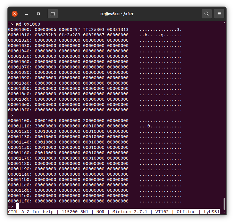
obviously the value at 0x1178 is 0x10000. As I mentioned before, you are reading an address from a table indexed by MSEL, and the figure in the docs tells you what the addresses in the table are.
Since the FU540 is open source, my thought is that this information is publicly available somewhere, but I can’t seem to find anything this detailed, just the user manual. I even tried the chip schematics just for kicks. Do you know if there are public documents with information as detailed as the memory contents of the jump table?
Are there some documents that aren’t released to the public? If the chip is designed so that memory address 0x1178 has the value 0x0001_0000 in it, that has to be documented somewhere.
The U54 core is open source. The FU540 SoC is not. Some parts, mainly analog stuff, is licensed. I don’t know if the mask rom is part of the core or not. If it is part of the core, then yes, it would be in the core sources somewhere. If it isn’t part of the core, then there would be no public sources for it.