Hi,
What would be the difference for PMU in handling the power on reset ( unplug the power / usb cable) and reset button push on board?
FE310 manual on page 72 PMU reset causes can be 0 - Reset and 8 - power on reset.
Hi,
What would be the difference for PMU in handling the power on reset ( unplug the power / usb cable) and reset button push on board?
FE310 manual on page 72 PMU reset causes can be 0 - Reset and 8 - power on reset.
@bsvtgc Table 42 of the Manual is a little bit unclear in this regard.
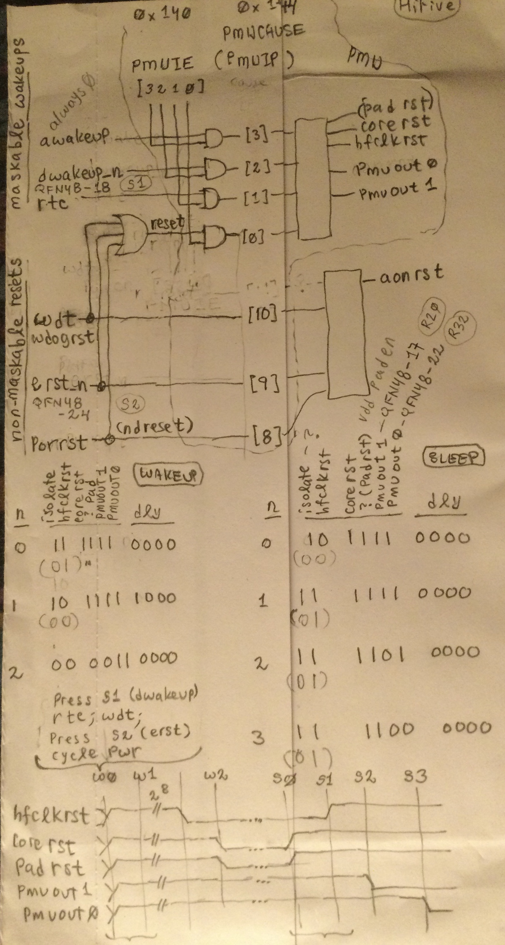
This table describes the ‘pmucause’ register, at offset 0x144.
The ‘pmucause’ field, which should actually be called ‘wakeupcause’, only applies to bits [2:0], and is further described in detail by detail Table 43.
The ‘resetcause’ field which is not shown (by mistake?) in Table 42, applies to bits [10:8], and is further described in detail by Table 44 – except for the first three lines which are a redundant copy/paste from the bits of the ‘wakeupcause’ field above.
All other bits of the ‘pmucause’ register, [7:3] and [31:11], are ‘reserved’ and unused.
Updated Tables 42, 43, and 44 of Chapter 15 of the Power Management Unit (PMU) are shown below.
Thus, to answer your question, the first (least significant) three bits of the ‘pmucause’ register tell what event woke up the chip. In the case of a reset event, shown by bit [0] being “H”, the higher-order bits (i.e., bits [10:8] of the ‘resetcause’ field) tell you whether it was a power-on event, External low-going pulse on the “ERST” pin (i.e. the reset button), or the watchdog got hungry.
Note that in case of wakeup from RTC (real time clock) or dwakeup, those three bits of the ‘resetcause’ field do not apply.
How to handle Reset::PowerOn or Reset::External is entirely up to how you arrange the wakeup and sleep program state machines in the PMU. By default (actually the Flash Recovery Mechanism program in OTP memory) the External Reset event generates a brief negative going pulse on the one of the two PMU signal pins – PMU_OUT_0 – for the purpose of completely unpowering the CPU core’s 1V8 supply.
With the Hi Five and also Lo Five boards the External mode of reset gives barely enough low-active time to completely power-off (i.e., disable) the VDD_1V8 regulator and thus completely reset the chip. This has to do with the very long 100K Ohm and 1 uF time constant and the voltage regulator’s input boas current on its digital control input Enable pin. This is talked about in the discussion of understanding the PRCI Clock Path and how reset handles the combination of the AON and PMU blocks and thus generates the PMU_OUT_0 signal to control power on/off in a less physical (than unplugging) way.
Hmm interesting. I would assume the reset causes be held in a AON register instead of PMU register. Figure 6 in FE310 manual, it looks like the reset cause is more of outside to PMU block in AON.
Okay, I see there isn’t any aon specific registers except aoncfg (can’t find much information about the AON block configuration information though)
True @bsvtgc while AON is where the various sorts of resets happen, they are sensed and reported in the sub-block of the PMU. This is presumably done so that basic functions of an analog nature (clock timings and voltage levels) come alive before any digital I/O (CPU, bus activity, etc) is engaged.
Think of AON as a “container” of other sub-blocks, of which there are six: WDOG, RTC, LFR, BackupRegs, PMU, and the AON itself. All of these six sub-blocks reside at the AON base address 0x1000 0000.
The PMU sub-block, for example, is configured with offsets 0x100 thru 0x14c.
Thus, the PMU diagram of Figure 8 of Chapter 15, and it’s register map in Table 37, fits nicely in the bigger picture inside the greater AON diagram of Figure 6 of Chapter 13, and its overall register map in Table 34.
You can see the actual circuit of the greater AON Block circuit diagram in its Scala documentation. You are right, I cannot find any mention of its aoncfg register (at offset 0x300); or for that matter, the bandgap measurement register, either.
The riscv-reset-path.png figure (in earlier message) shows how, on the HiFive board, an analog ERST input to the AON reset circuitry becomes a digital PMU_OUT_0 signal from the PMU sub-block.
Notice an interesting thing, that both of the internally sourced ring oscillators, HFR and LFR, are very similar in their construction – only their design parameters (i.e., number of inverter gates in their chains, and the propagation delays of each of those gates) are different, hence giving their different frequency ranges: KHz for the LFR, and MHz for the HFR. However, the LFR is at offset 0x7C of the AON’s base of 0x1000 0000, while the HFR is at offset 0x00 of the PRCI’s base of 0x1000 8000. This is noted in the PRCI chapter where LFR is described but referred later to the AON Chapter. This has always bothered me, it makes it difficult to organize the generic ring oscillator code stretched between two blocks and sub-blocks in an object-oriented way.
Those specific design parameters experimentally determined to be
HFR : a=11.558, b=35 (PRCI block base 0x1000 8000)
LFR : a=8.728, b=31 (AON block base 0x1000 0000)
with frequency of the ring oscillator defined given by the following equation
Hz = 1 / (a * (1 - (trim - 16)/b))
Where ‘trim’ is the five-bit value from 0 to 31 expressed as signed 2’s complement from -16 to +15.
A suggestion for a complete state machine model is shown in the prci.s file of my github repo at Demonstrating PRCI. There’s a tiny bug in my block diagram that I have not yet redrawn: the PLL post divider ‘d’ term is actually after the ‘pllbypass’ mux, not before it; and changing the value of ‘d’ does not in any way affect the state of PLL lock. You can think about ‘d’ and ‘outdiv’ together in the same sense.
Hello @pds your post is more clear than manual for PRCI. I find quite a few information is missing on PMU. For example the pmuie - PMU interrupt enables bits [0:2] how to interpret this field.
when read,
(gdb) x /x 0x10000140
0x10000140: 0x0000000b => How to interpret this?
(gdb)
Further, what would happen if pmusleep is initiated (unlock and pmuseep write) from debug-thru gdb mode ?
As per manual it should trigger sleep, but I doubt.
Hello @bsvtgc Think of register PMUCAUSE (0x144) as the “PMU_IP” (Interrupt Pending) analog of PMU_IE (0x140). Table 42 describes both of them, where bit 0 enables wakeup from reset events; bit 1 enables wakeup from rtc events; bit 2 enables wakeup from digital input (dwakeup_n, QFN48 pin 18, or Button S1 on HiFive board) events; and bit 3 enables wakeup from analog input (awakeup, presently not implemented, I think) events.
The value 0xb (0b1011) that you read from PMU_IE means reset, rtc, and awakeup will wake up a sleeping chip – and S1 button press dwakeup_n will not wake up the part.
Try setting (all bits of) PMU_IE to zero, writing 'KEY first of course. Then, nothing should wake up the chip once you PMUSLEEP (0x148) it, followed by writing KEY again. You would only be able to wake up the chip by cycling power. Setting PMU_IE to 0x4 would allow you to wake it up by pressing the S1 pushbutton (dwakeup_n).
In general, there are two kinds of events: maskable and non-maskable.
Maskable events are the wakeup signals, which you can enable or disable by PMU_IE.
Non-maskable events are the reset signals, which you cannot individually control – they are always enabled. However, you can disable wakeup from the all of the reset events by clearing bit 0 of PMU_IE. In this case only watchdog and ERST_n (HiFive button S2) will be disabled as long as power is applied. Cycling power off-then-on will cause all settings to revert back to their power-up states, thus poweron reset will be re-enabled and the chip will wake up. In other words, you can never disable the non-maskable poweron reset event.
What are the eight 32-bit values you read from gdb from PMUWAKEUPin (0x100 …); and what are the eight values you read from PMUSLEEPin (0x110 …)? The scala code seems to be a little different than the manual, in that bit 9 (isolate MOFF-to-AON power domain) is not defined, and the Flash Recovery Mechanism (FRM) code in OTP memory might have changed the wakeup and sleep “programs” of the PMU state machine from their poweron chip defaults. I am curious fo see what you read. These are the (eight, max) steps of the state machine programs. See lines 48-49 of PMU.scala, in the DevKitPMUConfig block.
The PMU state machine takes the four maskable events as inputs, and sequences them to generate the five outputs hfclkrst, corerst, padrsf, pmu_out_1, and pmu_out_0. Note that padrst is instruction bit [6], not shown in the Manual.
You can always watch with a scope on pmu_out_1 (QFN48 pin 17, HiFive R20) or pmu_out_0 (QFN48 pin 22, HiFive R32) to see if your PMUSLEEP command is taking effect. Perhaps it is, and something is immediately waking the chip back up again? Or, perhaps you’re not writing the right unlock code of 0x51F15E to PMUKEY (0x14C)? Remember that you have to write 'KEY every time you write any of the PMU registers (unlock state clears after each register’s write).
Here’s an idea: if you want to watch the wakeup (or sleep) process with a scope, you could change the PMUWAKEUP (or PMUSLEEP) programs so that you assert and deassert (i.e., pulse) either pmu_out_… line affer each step you assert or deassert the hfclkrst, corerst, or padrst; in other words, putting a handy external “marker” signal so you can observe these asynchronous events in a synchronous manner. Remember, however, on the HiFive and LoFive boards, pmu_out_0 is connected (through very long time constant) to the “EN” pin of the 1V8 regulator, which has effect of initiating a “poweron reset” event from CPU control. So you might not want to use it for marker purposes.
Hi @pds the default wakeup and sleep sequence matches as per manual. Minor correction though, the sleep sequence starts at 0x10000120 instead of 0x10000110 as you put above.
Default wake up sequence matches with the manual.
(gdb) x /x 0x10000100
0x10000100: 0x000003f0
(gdb) x /x 0x10000104
0x10000104: 0x000002f8
(gdb) x /x 0x10000108
0x10000108: 0x00000030
(gdb) x /x 0x1000010C
0x1000010c: 0x00000030
(gdb) x /x 0x10000110
0x10000110: 0x00000030
(gdb) x /x 0x10000114
0x10000114: 0x00000030
(gdb) x /x 0x10000118
0x10000118: 0x00000030
(gdb) x /x 0x1000011C
0x1000011c: 0x00000030
Default sleep sequence:
(gdb) x /x 0x10000120
0x10000120: 0x000002f0
(gdb) x /x 0x10000124
0x10000124: 0x000003f0
(gdb) x /x 0x10000128
0x10000128: 0x000003d0
(gdb) x /x 0x1000012C
0x1000012c: 0x000003c0
(gdb) x /x 0x10000130
0x10000130: 0x000003c0
(gdb) x /x 0x10000134
0x10000134: 0x000003c0
(gdb) x /x 0x10000138
0x10000138: 0x000003c0
(gdb) x /x 0x1000013C
0x1000013c: 0x000003c0
I will take some time to soak with the data you have provided and try to scope the PMU EN pin. Your idea to scope the PMU EN pin is an easy way to test wake/sleep sequence and confirm if all configuration is correct and should precede my test to put the core to sleep and wake up after button press.
Thanks @bsvtgc great info! Note that this particular sleep sequence affects both of the pmu_out_ pins, so you have two things you can look at.
First, at the third sleep step (#2; 0x128; the 0x3D0 instruction) you will see pmu_sleep_1 drop to logic “L”. You can probe this signal at R20, it’s called WF_RESET.
Then, at the fourth sleep step (#3; 0x12C; the 0x3C0 instruction) you will see pmu_sleep_0 drop to logic “L”. You can probe this signal at R32, it’s called VDD_CORE_EN. If you probe the downstream side of R32, or its destination at the 1V8 regulator U8-3, you’ll see a weird waveform with huge time constant; it’s normal and as expected. I’d suggest looking at the upstream (SoC) side for now.
Here is a quick sketch of everything I mentioned earlier, to help seeing the bigger picture. State machine execution time, the interval between each of the eight Wakeup or Sleep steps, is, of course, determined by the setting of the LFR oscillator…
My apologies @bsvtgc I was a little bit mis-stated about PMUCAUSE register above.
One sentence in Section 15.7 of the Manual gives it all away
The value in the
wakeupcausefield corresponds to the bit position of the event in pmuie.
That “correspondence” is explained in the PMU.scala code at lines 64 and 76, with use of the log2Ceil() function.
resetCause = UInt(INPUT, log2Ceil(new ResetCauses().getWidth))
wakeupCause = Reg(init = UInt(0, log2Ceil(c.nWakeupCauses)))
In other words, that correspondence means the individual bits of the PMUIE register are seen as a decimal value of the PMUCAUSE register. It is further evident in the Manual with the use of the word “Bits” versus the word “Index” in the various tables describing this register. I overlooked that subtle hint in my previous explanation above.
Further, line 115 of the PMU.scala code explains precisely what’s missing in Table 42 of the Manual. The values of the wakeupcause field begin at bit position 0; and the values for the resetcause field are placed beginning at bit position 8.
io.regs.cause.read := wakeupCause | (io.resetCause << 8)
Table 42, describing the PMUCAUSE register, should read like this. Note the difference between Bits and values.
Bits    Field Name    Description
[7:0]   wakeupcause   PMU Wakeup Cause values
[15:8]  resetcause    PMU Reset Cause values
[31:16] Reserved
Then, Tables 43 and 44 look like these:
Table 43: Wakeup cause values
Index  Meaning
0      Reset wakeup
1      Real time clock timer wakeup
2      External wakeup (dwakeup_n pin)
3      External wakeup (awakeup pin, someday)
4-15   Reserved
The reference for Table 43 is at lines 11-16 of PMU.scala.
Table 44: Reset cause values
Index  Meaning
0      Power-on reser
1      External reset (erst_n pin)
2      Watchdog timer reset
3-15   Reserved
The reference for Table 44 is at lines 18-22 of PMU.scala.
In general, the PMUCAUSE register does not resemble “interrupt pending (ip)” as I postulated earlier. The PMUCAUSE register instead functions more like a “cause” field, in the same sense as that of the synchronous exceptions and asynchronous interrupts (i.e., when handling and decoding mtvec events); of the internal software and timer interrupts of CINT and CLINT (such as MTIMECMP); or the peripheral interrupts of the PLIC.
We can decode PMCAUSE events and their values something like this, which you can invoke at _start (or, _startup) with a jal pmu_cause_handler call (or simply j if you don’t wish to return from there). The .weak directives allow you to override these trivial handler tail functions with more sensible implementations elsewhere and marked with the .global directive. You might put this handler in a file called pmu.s, parallel to other files called clint.s and plic.s, which contain clint_trap_handler and plic_trap_handler, respectively; so that your start.s file can remain suitably general, short, and sweet.
pmu_cause_handler: .global pmu_cause_handler
  li AON_BASE
  lw a0, AON_PMUCAUSE(t0)
  andi t1, a0, 0x3   # decode 0,1,2,3 only
  slli t1, t1, 2     # four-byte table entries (or two bytes for compressed j's)
  la t2, pmu_wake_vectbl
  add t2, t2, t1
  jr t2

pmu_wake_vectbl:
  j pmu_wake_rstvec  # PMUIE[0]=pmurstie, aggregate (wire-or) of reset sub-causes
  j pmu_wake_rtcvec  # PMUIE[1]=pmurtcie
  j pmu_wake_digvec  # PMUIE[2]=pmudigie, QFN48-18, HiFive button S1
  j pmu_wake_anavec  # PMUIE[3]=pmuanaie

pmu_wake_rstvec:
  srli t1, a0, 8     # sub-decode [15:8]
  andi t1, t1, 0x3   # decode 0,1,2,3 only
  slli t1, t1, 2     # four-byte table entries (or two-bytes for compressed j's)
  la t2, pmu_rst_vectbl
  add t2, t2, t1
  jr t2

pmu_wake_rtcvec: .weak pmu_wake_rtcvec
  ret   # or j, as desired

pmu_wake_digvec: .weak pmu_wake_digvec
  ret   # or j, as desired

pmu_wake_anavec: .weak pmu_wake_anavec
  ret   # or j, as desired

pmu_rst_vectbl:
  j pmu_rst_pwronvec
  j pmu_rst_erstvec    # QFN48-24, HiFive button S2 (LoFive button S1)
  j pmu_rst_wdtvec
  j pmu_rst_xxxvec

pmu_rst_pwronvec: .weak pmu_rst_pwronvec
  ret   # or j, as desired

pmu_rst_erstvec: .weak pmu_rst_erstvec
  ret   # or j, as desired

pmu_rst_wdtvec: .weak pmu_rst_wdtvec
  ret   # or j, as desired

pmu_rst_xxxvec: .weak pmu_rst_xxxvec
  ret   # or j, as desired
The PMU Wakeup interrupt enable bits look like the following. Lines 51-58 of PMU.scala describe exactly how the bits of the PMUIE register follow exactly the same order as those of wakeupcause, of course as bits, not values.
ie = new SlaveIF(c.nWakeupCauses)
Table 41 of the Manual should look like this:
Table 41: PMU Wakeup Interrupt Enable
Bits   Field Name    Description
0      pmurstie      Reset wakeup enable
1      pmurtcie      RTC comparator wakeup enable
2      pmudigie      dwakeup_n pin wakeup enable
3      pmuanaie      awakeup pin wakeup enable, someday
[31:4] Reserved
Lastly, notice Section 7.3 of the Manual which describes the Sleep Mode and the wakeup process and sequence of steps of the default PMUSLEEP[0…7] program. Paraphrasing slightly,
… turn on core & pad power; wait for power to stabilize; deassert clock reset; deassert core & pad reset; begin (continue) execution from reset vector 0x1004. after wakeup, the clock runs from internal HFROSC at its default
trimanddivsettings.
Thus, from Run Mode, a wfi instruction enters the Wait Mode where clocks remain running but disconnected from the core, and states are preserved; and an enabled CLIC, CLINT, or PLIC interrupt returns back to Run Mode, with the mret instruction.
Similarly, from Run Mode, writing PMUSLEEP (preceded by writing PMUKEY) enters Sleep Mode through a sequence of steps dictated by the PMUSLEEP(0…7) program; and an enabled PMU Wakeup interrupt returns back to Run Mode, starting at 0x1004, through another sequence of steps dictated by the PMUWAKEUP(0…7) program.
@pds Thanks for your inputs & corrections, I haven’t yet gone to wakeup, tried with pmusleep and got it working with quick/short code as below: Will try to wake up soon.
; Unblock PMU
li t0, AON_BASE;
li t1, PMU_KEY;
sw t1, PMU_KEY_OFST(t0);

#set pmuie to 0
sw zero, PMU_IE_OFST(t0);

; Unblock PMU
sw t1, PMU_KEY_OFST(t0);

;set to sleep - any value
li t1, 2;
sw t1, PMU_SLEEP_OFST(t0);
setting pumie to 0, prevented it from waking up and debugger lost control of the core. This is due to the sleep sequence instructions on bits [4:5] are from 11 → 01 → 00
0x10000120:     0x000002f0   pmusleepi0
0x10000124:     0x000003f0   pmusleepi1
0x10000128:     0x000003d0   pmusleepi2
0x1000012c:     0x000003c0   pmusleepi3
0x10000130:     0x000003c0   pmusleepi4
0x10000134:     0x000003c0   pmusleepi5
0x10000138:     0x000003c0   pmusleepi6
0x1000013c:     0x000003c0   pmusleepi7

bit[4]  corresponds to pms_out_0_en  (VDD_CORE_EN)
bit[5] corresponds to pmu_out_1_en  (WF_RESET)
bit[4] pms_out_0_en => VDD_CORE_EN controls the 1.8v output, cutting off the power to core right after first 3 instructions of sleep sequence and when scoped WF_RESET too at R20, it goes from LOW to HIGH and then finally to low after.
This ensures that the pmusleep works. Will try soon to wake with RTC once I configure RTC.
Meantime I wonder about the bit[9] - isolate in PMU instruction format. it’s always set during the sleep sequence and what would happen if it’s unset? Does unset mean there won’t be any separate clock & power domain between AON & MOFF?
Also, you reminded me of the “wait mode” in your reply another mode pending to try.