Hi @bsvtgc how did you get your value of 12? I calculate the divisor as 13,800,000 Hz / 115,200 bps = 119 (truncated, rounded down).
Note that the value you store in the DIV field of register offset 0x18 is one less than this calculated value, in other words, 118 in this case of the 13.8 MHz clock rate.
To probe the internal tlclk (or, hfclk) signal at the outside world, you can configure and enable any one of the three PWM blocks, and look at the PWMx.0 pin of that block.
Hi @pds I am trying to decode the clock hfclk value at reset. With the reset values at registers, I am able to arrive at the following picture. But what is the default value of psdclkbypasss_n ?? The red highlighted line is the default clock source.
so if psdclkbypasss_n =1, then hfclk = 13.8 Mhz. Would you be able to confirm the psdclkbypasss_n value at reset?
HI @bsvtgc nice picture. Admittedly, Figure 3 of Chapter 6 of the (FE310-G002) Manual is a little bit unclear about selector line for the last mux in the clock path of the PRCI block. Here is a slightly improved diagram:
As you can see, the internal psdclkbypass_n signal is actually exposed through an inverter to pllbypass, which is bit [18] of register PLLCFG (0x10008008).
Thus, pllbypass=1 (which is the power-on reset state, as shown in Table 9 of Chapter 6) means internally psdclkbypass_n=0, which selects the direct (non-pll’d) path from the external crystal input source. This setting also turns off power to the PLL.
The SoC cannot operate at power-up without an external crystal or oscillator attached to the hfx pins.
If you want to switch to using the internal (ring) oscillator, and observe your hfroscout (and, thus, hfclk) value of ~13.8 Mhz, first set hfroscen=1 and pllsel=0 (both of which are the states at power-up), then wait for hfroscrdy to be ‘1’, and lastly set pllbypass=0 (which means internally psdclkbypass_n=1).
It is interesting that you cannot run the hfr internal (ring) oscillator without also having the PLL enabled. It is unclear to me exactly what happens when the PLL has no pllref input or its configuration settings are set to invalid values.
@pds Thank you, that clears the power-on core & tl clock settings which in-turn supplies the UART.
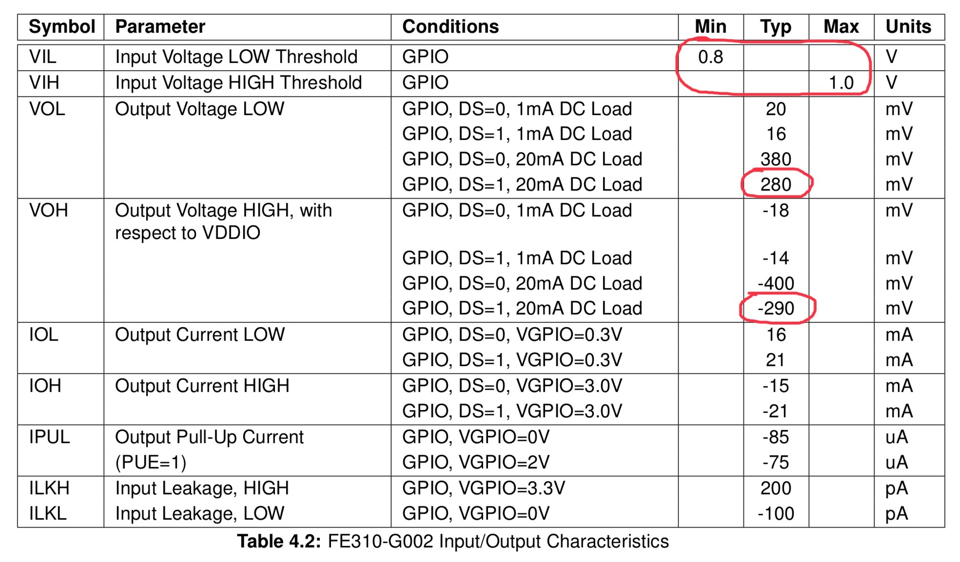
On the UART pin voltage thresholds, the data sheet Table 4.2 has the following values.
UART Rx side (V in low min) = 0.8 V
UART Rx side (V in low max) = 1 V
On the Tx side, I could n’t find what DS=0, and DS=1 mean?
with 20mA DC load (taking DS=1):
UART Tx Side (V out Low typ) = 0.28 V
UART Tx Side (V out High typ) = 3.01V (3.3 - 290mV)
Are above derived values correct?
I understand the actual range might differ & I read the disclaimer on top about the electrical characterics. But I am trying to ensure if I read the data sheet properly. coz, I read the conditions column mention GPIO alone. Would this vary if that GPIO is configured as IO/UART?
I am planning to use GPIO 18 (UART1 TX) & GPIO 23 (UART1 RX) and see if I can make it work with loopback with Hifive1-Rev B board. I see UART 1 is free to use in hifive1-revb.
You are correct, @bsvtgc, about the pin voltages in Table 4.2 of the Datasheet. I couldn’t find the reference to the “UART” specs you mentioned, but they are the same as in Table 4.2:
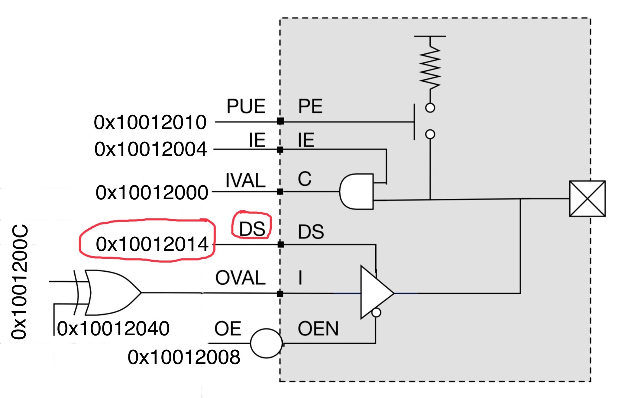
The DS setting is the Drive Strength register of the GPIO block. When the appropriate UART Tx (i.e., outpudt from SoC) bits are logic ‘1’ there is about 5 mA more current available.
The GPIO pin control registers control settings of the physical I/O pins regardless of any I/O Function mode.
For your UART test, control the output Tx drive strength (depending on load from other side of the serial link) with 0x10012014 |= (1 << 18).
Also for your UART test, depending on the driving capability from the other side of the serial link, or if there’s an electrically noisy environment, you might also want to engage the input pin pull-ups: 0x10012010 |= (1 << 23).
Note that the Output XOR register (0x10012040) functions regardless of any I/O pin mode – you might want to make sure the relevant bits are in default ‘0’ (non-invert) state for proper IOF operation of the output lines for those peripherals.
You have brought up a very good point @pds on the pull ups.
I understand pull up on Rx side, but UART tx line should be pulled high prior start bit, followed by data bits and stop bits and then raised high to mark the end of transmission as part of the protocol. For Uart Tx pin, these internal pull up are n’t needed, right?
Also, keeping UART rx aside, the drive strength to send “1” on UART tx line should be 8 mA IIVDD from Table 4.1 at 16Mhz. right? How this drive strength (IIVDD from Table 4.1) differs from the DS at GPIO pin corresponding to UART tx?
Table 4.1 (of the Datasheet) specifies supply current for the entire SoC overall, not just the UART device, I think.
Initial conditions of the Rx lines generally are responsibility of the driving (Tx) source on the other end of the serial link, so receiving end pull-ups probably have little effect. I’m sure that, even with PUE=0, the GPIO block inputs already have some background pull-up current.
From Chapter 17, Section 8 of the Manual there is this reminder that direct software control of some pin functions might be unavailable:
When a pin is set to perform an IOF, it is possible that the software registers [input_val/output_val] port, output_en, pullup, ds, input_en may not be used to control the pin directly. Rather, the pins may be controlled by hardware driving the IOF. Which functionalities are controlled by the IOF and which are controlled by the software registers are fixed in the hardware on a per-IOF basis. Those that are not controlled by the hardware continue to be controlled by the software registers.
Thus, in case of the UART’s, it could be that DS and PUE are both fixed at their default values (‘0’) and not controllable.
Further inspection of the GPIO block IOF and the device peripheral UART circuitry is probably necessary. Actual hardware test experiment to check UART operation while changing the settings of DS and PUE might be a good idea, too.
Last, note that “IE” for the GPIO block and I/O pins means Input Enable, not Interrupt Enable as for UART, SPI, and the other blocks.
@pds I am back again with no luck on UART transmission on UART 1 tx pin.
Following are the things I did.
Set the priority of all interrupt sources (except src 4 corresponding to UART 1 ) to priority 2 at PLIC
and set UART 1 source 4 priority to 3.
Set the PLIC priority threshold to 2 (to mask all interrupts except UART 1)
Configure GPIO18 (UART 1 tx) as IOF
Enable machine external interrupt
Enable interrupt source id 4 at PLIC
Set the divisor register to 512 (baud rate of 115200 at 16Mhz)
Set the tx water mark level to 3
Configure 2 stop bits (8-N-2)
Enable UART 1 tx in control register
Keep sending 0xaa in a loop
I verified all the above settings are in reflecting in the CSR & MMIO registers.
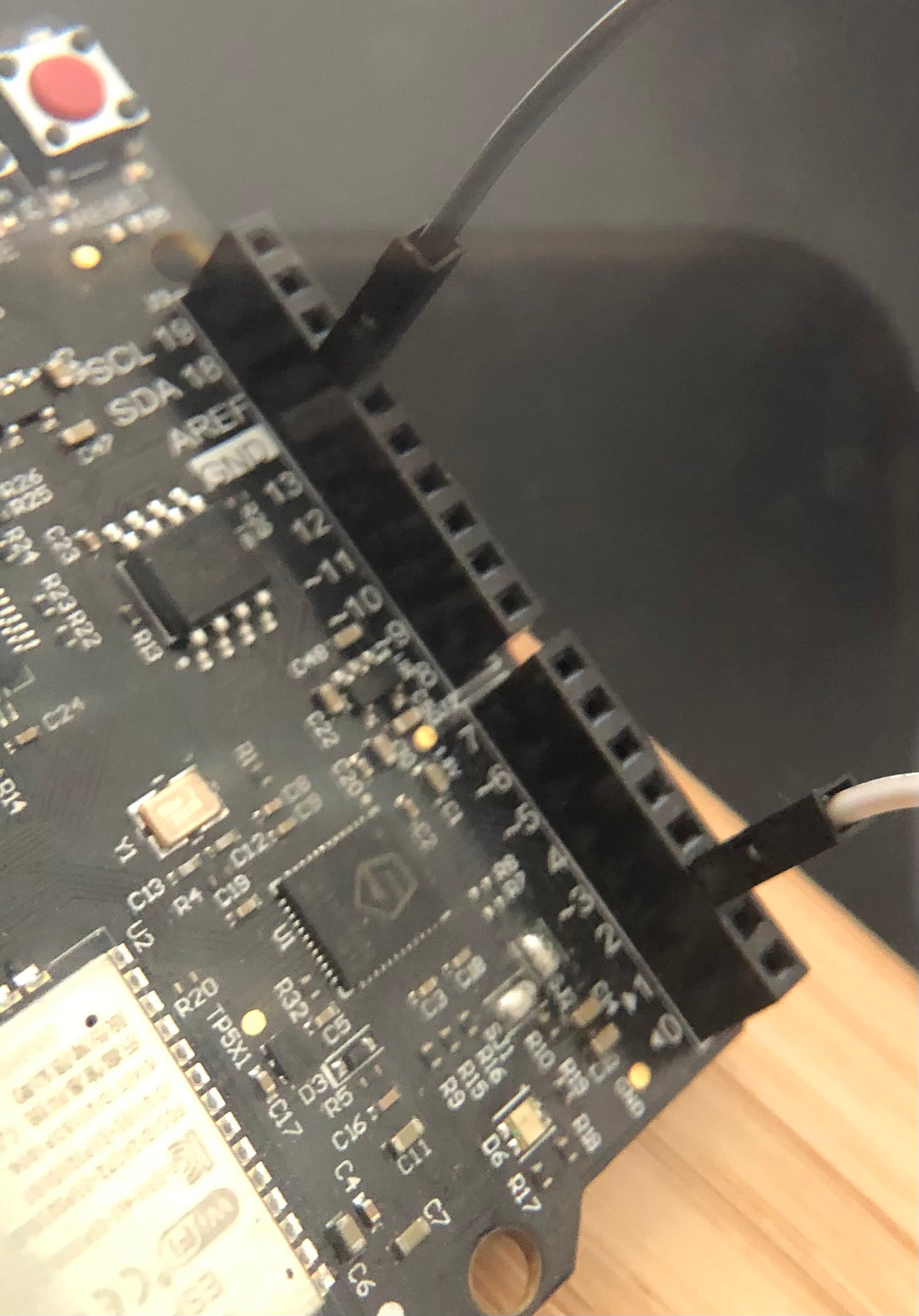
But neither interrupts are generated (I expect water mark interrupts) nor I see high and lows at the UART 1 tx pin. I probe at GPIO 18 on J2 jumper on board.
@bsvtgc hmm, interesting. Try it first in direct code without interrupt handling. Are you setting up both IOF_SEL and IOF_EN in your 3rd step? If the IOF_EN bit is not set, it might explain why you see no activity on the tx (output) pin.
@pds Little progress, able to receive the interrupts for UART 1.
Thanks to your input, I missed to enable the gpis_iof_sel. Also, when I copied the div value from the table in manual, I copied 512 (corresponding to baud 31250 in above row) & now I corrected it to 138.
But still I don’t see any activity on the UART tx (gpi0 18 ) pin. In this regard;
I follow schematics B01 dated 4/11/2019 sheet 3 for hifive1-revb board. Schematics numbering of J2 jumper don’t match actual board rev B01. I am NOT sure if you have the same board. In schematics, the numbering run from 1 to 8, whereas in actual board it run from 0 to 7. I am probing at #2 on board.
Would you be able to confirm if this #2 on J2 jumper is the UART 1 tx?
Also the order my code is enqueue 3 bytes, enable UART, then inside loop keep sending bytes without any delay. I don’t know what would happen when FIFO is full. What would be the right way of doing it?
Wait for water mark interrupt, inside interrupt routine, enqueue x bytes equal to water mark depth and then do the same for every water mark interrupt?
Yes, @bsvtgc, admittedly the silkscreen labeling of the board is a little cryptic. On the schematic, Arduino-like connector J2’s lines are real, physical pin numbers, they always start from ‘1’ of course; the logical naming of signals starts with ‘0’. Glad you got the right idea.
Interesting to me why you only work with one (Tx) side of the UART? Try also selecting and enabling the I/O Function (using IOF_SEL and IOF_EN), respectively, and enabling the device block (using RXCTRL) for the Rx side as well.
If you do this, you can then connect together GPIO’s 18 & 23 (J2 pins 3 & 8, which are PCBA silkscreen labels 2 & 7) to make a complete functional link in a loop-back sense. You might then see some electrical activity.
@pds Though loopback would be normal way to start, I didn’t since I wanted to capture the activity on my scope (saleae ) . I wasn’t sure if possible to loopback through scope would work. Hence started only to transmit and see if I can capture.
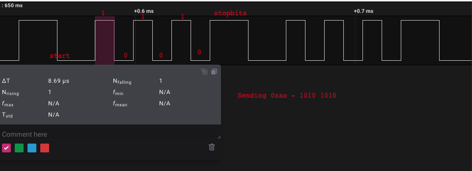
With 8-N-2 at 115200 baud rate, and sending 0xaa, the waveform seems okay except missing a bit.
Duration of each bit ~ 8.69microsecs (correct with baud 115200)
2 stop bits correct with the configuration.
But the waveform don’t match with 1010 1010 (0xaa). Any clue @pds ?